










- Windows
- Prisms
- Spherical Lenses
- Cylindrical Lenses
- Mirrors
- Beamsplitters
- Polarization Optics
- Singlet True Zero Order Waveplate
- Cemented True Zero Order Waveplate
- Cemented Zero Order Waveplate
- Optical Contact Zero Order Waveplate
- Air-Spaced Zero Order Waveplate
- Low Order Waveplate
- Multi-Order Waveplate
- Narrow Band Polarization Beamsplitter Cube
- Broadband Polarization Beamsplitter Cube
- Rotator
- Glan Taylor Polarizer
- Glan Laser Polarizer
- Glan Thompson Polarizer
- Glan Thompson Polarization Beamsplitter Cube
- Wollaston Polarizer
- Rochon Polarizer
- Broadband Polarization Beam Combiner
- Brewster Polarizer
- Brewster Window
- Coatings






Two-dimensional semiconductors offer a promising route toward ultra-low-threshold nanolasers. Researchers at the Suzhou Institute of Nano-Tech and Nano-Bionics, CAS, have designed a twisted photonic crystal nanocavity. Heterogeneously integrated with monolayer tungsten disulfide, the device demonstrates stable lasing under room-temperature continuous-wave optical pumping and sets a new record for the lowest room-temperature threshold among 2D semiconductor lasers.
The team fabricated two finite hexagonal photonic crystals on a thin silicon nitride membrane and rotated them at a selected angle. This twist creates a quasi-continuous radial gradient in air filling fraction across unit cells, producing a radially varying bandgap. Functioning like precisely nested concentric mirrors, this graded bandgap tightly confines light modes within the central air region to form an extreme air mode. In this configuration, most of the optical field resides in air and overlaps efficiently with excitons in the suspended monolayer WS₂. Excitons emit light efficiently in the suspended region, eliminating dielectric screening and non-radiative quenching at dielectric interfaces.
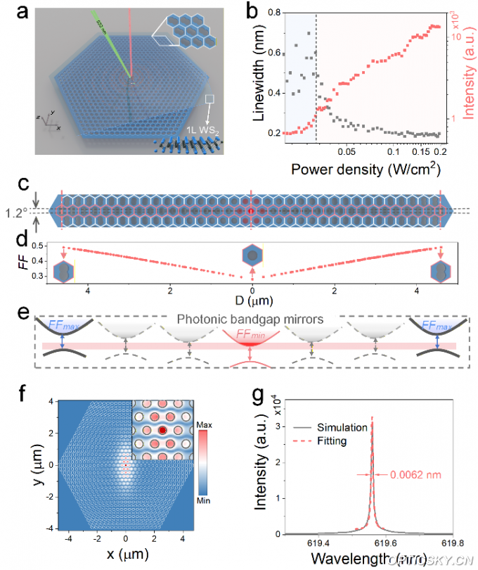
Operating principle of the two-dimensional semiconductor laser
The nanocavity achieves an ultra-small mode volume of only 0.36(λ/n)³ and a simulated quality factor up to 100,000. Lasing is realized in monolayer WS₂ under room-temperature continuous-wave pumping at an extremely low power density of 0.03 W/cm², establishing a new threshold benchmark for 2D semiconductor lasers. This breakthrough opens a new avenue for ultra-low-power on-chip light sources.
The findings were published in *Advanced Materials*. The research was supported by the National Key R&D Program and the National Natural Science Foundation of China.